Thank You For Purchasing The RFID Receiver Test Kit
In this kit we'll focus on the RFID 'receiver'. The RF receiver is the heart of this Kit. The receiver implements techniques used in transistor radio receivers applied at 125kHz.
Theory of operation:
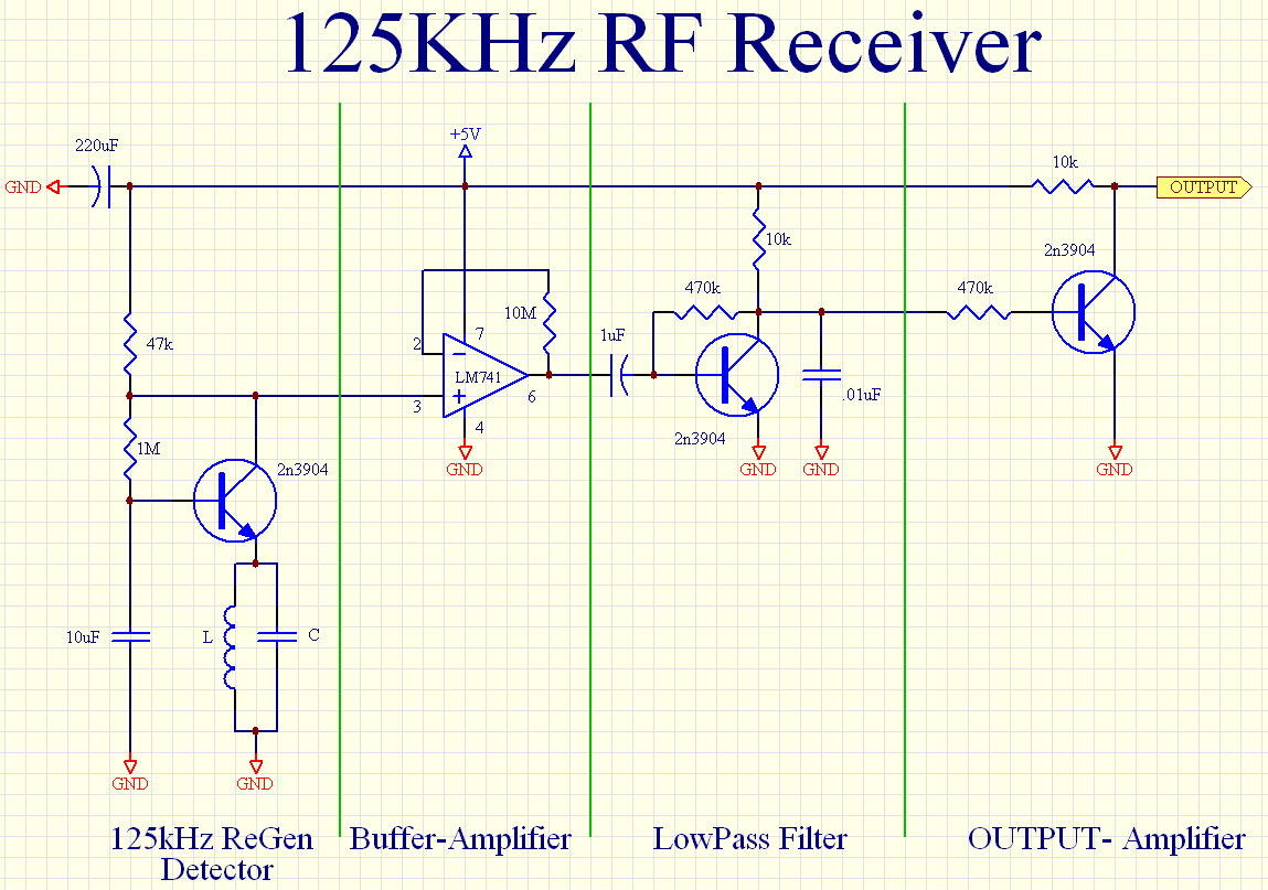
The L/C are selected to form a resonant tank circuit tuned to about 125kHz. These values are approximately 33uH for L and 0.047uF for C. The 10uF capacitor is trickle charged through the 1M and 47k resistor from the 5V supply. When the capacitor reaches the turn-on voltage for the transistor, the transistor begins to conduct, allowing the ground (GND) to influence the collector. This ground influence causes the positive voltage turning ON the transistor to be quenched. As a result an equilibrium is established in the most sensitive linear region of the transistor. Because of where the L/C tank is located the Collector of the transistor becomes an Emitter follower, meaning that anything that happens at the Emitter of the transistor is also seen at the Collector of the transistor in the same phase. The phase relationship here is very important because it provides re-enforcing feedback to the L/C tank through the B-E junction of the transistor. i.e. as the Emitter becomes positive the transistor turns off, this allowing a small portion of the +5V supply the feed through the 47K and 1M resistor into the Base-Emitter junction and to the L/C tank in the same polarity phase. This unique transistor feedback creates what is called a “Q”multiplier and provides several thousands of times more amplification that a single transistor would normally be capable of doing. The benefit of a “Q”multiplier is to dramatically increase your signal to noise ratio. During the multiplication, because of the tuned LC tank, random fluctuations to not get re-enforced, while any signal that is within the L/C tank frequency is re-enforced. This is also known as a re-generation circuit. Typically a re-gen circuit requires a tickler coil and/or a reflex coil. In this case the reflex coil is also the L/C tank. So now that we have this HUGE amount of amplification, the impedance is still very high, so we need to buffer. An Op-Amp was selected because of it's typical off-the shelf availability, and despite the 10Meg resistor for the buffer feedback, the high impedance of the Detector stage only makes the total gain about 5x at this stage. The next stage is a low pass filter. The goal here is to remove the 125kHz component. This sounds counter intuitive, because after all that's the very frequency we are tuning. However 125kHz is actually the carrier frequency, the real data is modulated within the 125kHz carrier. So applying a low pass filter leaves us with just the modulated signal without the 125kHz. This is simply done by placing a capacitor across the Emitter-Collector junction of the transistor. The final stage is just to clean up the signal so that it is more compatible with a micro controller interface.
RFID receiver schematic:
RFID receiver Parts List:
x1 1Meg resistor (Brown-Black-Green)
x1 1uF capacitor
x2 10k resistor (Brown-Black-Orange)
x1 10Meg resistor (Brown-Black-Blue)
x1 10uF capacitor
x1 220uF capacitor
x3 2n3904 transistor
x1 3-Pin SIP connector
x1 33uH Coil with 0.047uF Capacitor
x1 330 Ohm resistor (Orange-Orange-Brown)
x1 47k resistor (Yellow-Purple-Orange)
x2 470kresistor (Yellow-Purple-Yellow)
x1 8-DIP socket
x1 Blue LED
x1 LM741CN Operational Amplifier
x1 PCB board
Tools you will need:
Soldering Iron
Solder
wire cutters (A spare pair of finger nail clippers works well)
wire strippers
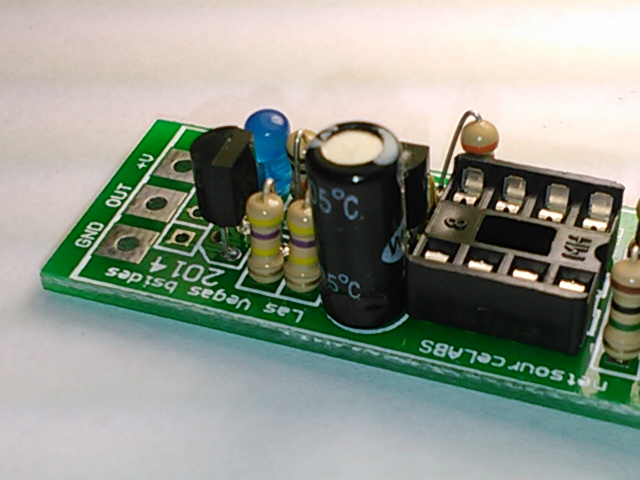
Step 1:
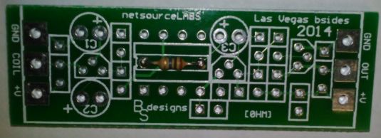
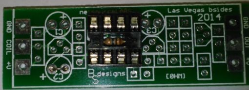
Identify the PCB you will be assembling by the silkscreen printed on the PCB.
Step2:
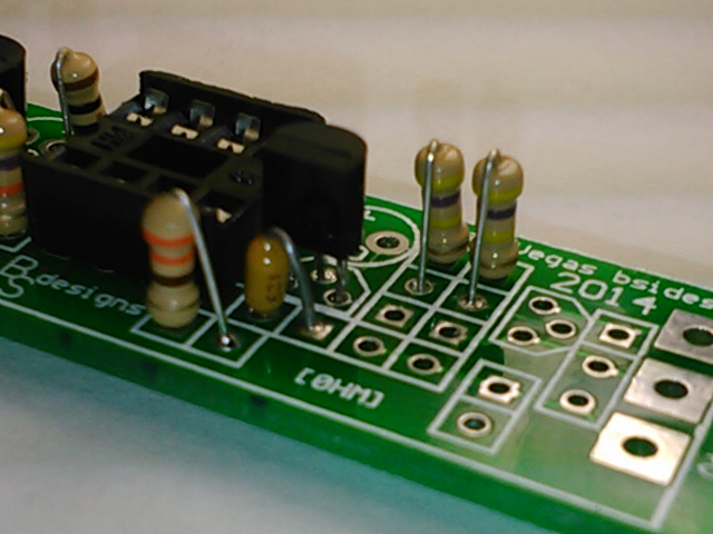
Place the 10Meg (Brown-Black-Blue) resistor on the PCB. Trim the excess leads as necessary. Note: This resistor should have as short of leads as possible and can either go on the top side of the board or the bottom of the board. It is meant to go under the 8-Pin DIP socket (top side) which we will be installing later. Save at least one of the trimmed resistor leads for an errata we will do in the next step.
Step3:
C2 has been omitted and needs to be shorted with a jumper instead. From Step 2 if you saved one of the 10Meg resistor leads you can use that to make a jumper.
Step4:
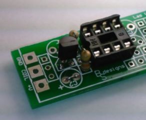
Place the 8-Pin DIP socket on the PCB. Note: Take notice to orient the dimple on the PCB silk screen with the dimple of the physical socket. It may be hard to tell unless you look really close because of the resistor silk,but the dimple should point to the left if the board is oriented so that the writing is right side up.
Step5:
Place the 1Meg resistor (Brown-Black-Green) on the PCB. Trim the excess leads as necessary. Note: bend leads so that the resistor will stand up perpendicular to the board when soldered.
Step6:
Similar to Step5, Place a 47k resistor (Yellow-Purple-Orange) on the PCB. Trim the excess leads as necessary.
Step7:
Place one of the three 2n3904 transistors on the PCB. Note the orientation of the transistor to the silkscreen, and slightly bend the middle pin on the transistor (The BASE) toward the round side of the transistor in order for it to fit in place. Trim the excess leads as necessary.
Step8:
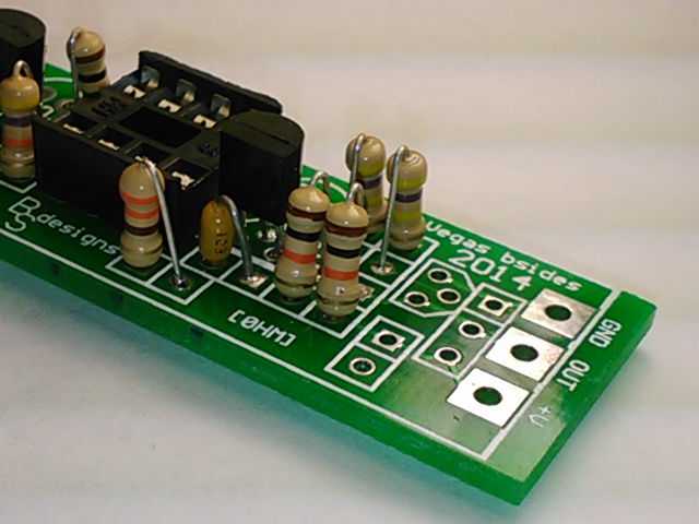
Place a 330 ohm resistor (Orange-Orange-Brown) on the PCB. Trim the excess leads as necessary.
Step9:
With a similar theme, place the .01uF capacitor (103) on the PCB and bend the leads so that it will stand perpendicular to the BCP when Soldered.
Step10:
As in Step7, place the second of the three 2n3904 transistors on the PCB. Note the orientation of the transistor to the silkscreen, and slightly bend the middle pin on the transistor (The BASE) toward the round side of the transistor in order for it to fit in place. Trim the excess leads as necessary.
Step11:
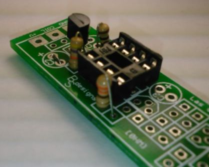
Place both 470k resistors (Yellow-Purple-Yellow) on the PCB. Trim the excess leads as necessary.
Step12:
As in Step11, place both 10k resistors (Brown-Black-Orange) on the PCB. Trim the excess leads as necessary.
Step13:
As in Step7 and Step10, place the last of the three 2n3904 transistors on the PCB. Note the orientation of the transistor to the silkscreen, and slightly bend the middle pin on the transistor (The BASE) toward the round side of the transistor in order for it to fit in place. Trim the excess leads as necessary.
Step14:
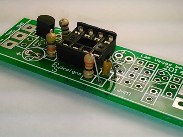
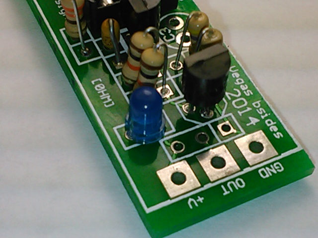
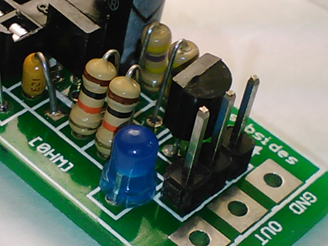
Place the blue LED on the PCB. Trim the excess leads as necessary. Note: LED's have a polarity, the longer lead is the Cathode (+) while the shorter lead is the Anode (-). The longer lead in this circuit needs to go towards the top of the board if the board is oriented so that the writing is right side up.
Step15:
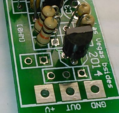
Place the 1uF capacitor on the PCB. Trim the excess leads as necessary. Note: Capacitors have a polarity with the negative terminal usually indicated. Observe the polarity on the silkscreen (indicated with a '+' for the positive terminal)
Step16:
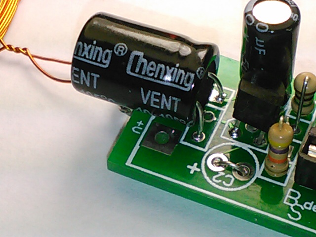
Place the 10uF capacitor on the PCB. Trim the excess leads as necessary. Note: Capacitors have a polarity with the negative terminal usually indicated. Observe the polarity on the silkscreen (indicated with a '+' for the positive terminal)
Step17:
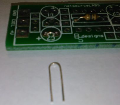
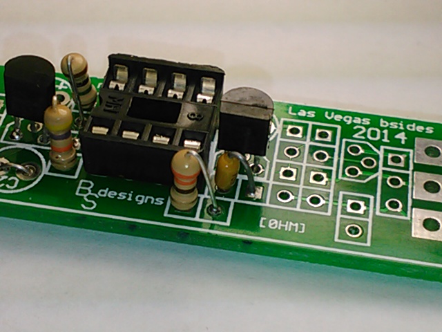
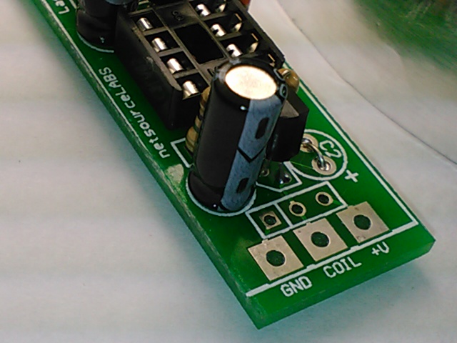
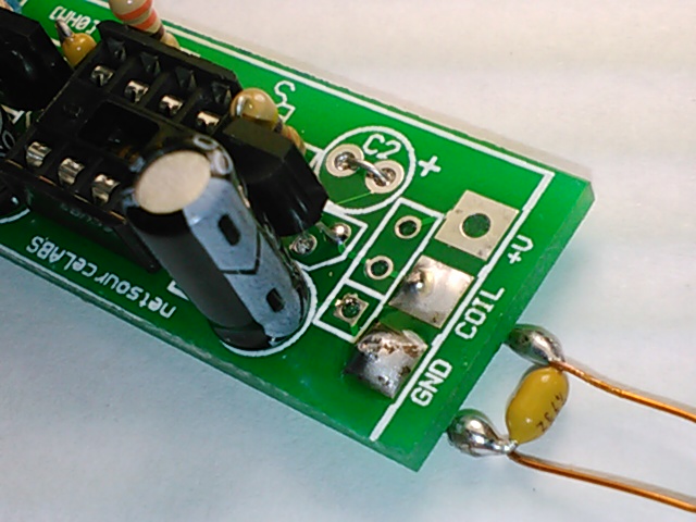
Place the 33uH coil and 0.047uF capacitor (The L/C tank) to the back side of the PCB via the GND and COIL terminal. Trim the excess leads as necessary.
Step18:
Place the 220uF Capacitor on the PCB. Trim the excess leads as necessary. Note: Capacitors have a polarity with the negative terminal usually indicated. This connection is an errata and is not indicated by the silkscreen. The positive terminal should connect to the 3pin SIP pin that is closest to +V, while the negative terminal should connect to the 3pin SIP pin that is closest to GND.
Step19:
Place the 3-Pin SIP connector on the PCB.
Step20:
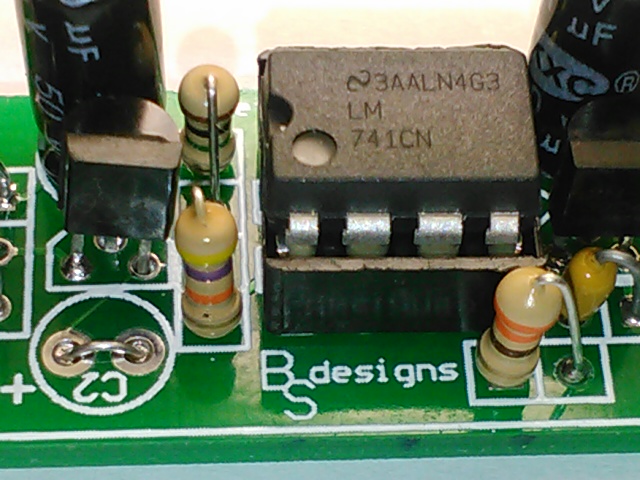
Carefully insert the LM741CN into the 8-Pin DIP socket. Make Note of where the dimple on the IC is in relation to the socket. Make sure that all of the pins of the IC are aligned with the socket and gently press the IC into the socket. This may require some slight bending of the IC pins in order to achieve proper positioning.
Step21:
Congratulations!!! You are ready to apply power for testing, and if you have completed the first part of this kit, you have the RFID 'exciter' ready to go.
If you have a scope, or have software on your PC to analyze the data then you should see something similar to this on the OUT pin on the RFID detector PCB when a RFID tag is placed on or near the RFID exciter coil. This output is the RAW modulated output from the RFID receiver where no signal decoding has been applied. You can take the signal from here and apply your own decoding scheme for cards outside of the scope of the EM4100 protocol.
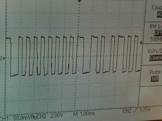
Note: This circuit is a sensitive RF amplifier, and is susceptible to interference, and consequently there is a lot of noise at the 125kHz end of the spectrum. If there are any fluorescent lights near the receiver or if the receiver is too close to a computer monitor it can cause interference problems.
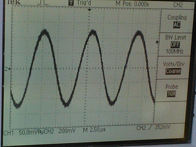
For another test point, you can try removing the LM741 and probing the 8-DIP socket on pin #3. This location will provide the output directly from the “Q”multiplier circuit and the output should look something like this...
Shielding can also make a huge difference. A single ground plane is enough for this circuit. What I have done is to take a business card with Aluminum metal foil adhesive and attached that to the card while a wire connection from the metal foil goes to ground.
Step22:
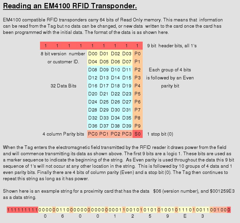
Going further !! The next portion of the kit allows us to audibly “hear” what's going on at 125kHz and decode the Manchester encoding from a standard EM4100 RFID tag. The EM4100 Protocol is outlined below...